 Edited by
Short answer
A GPU is a general-purpose parallel processor with matrix units (Tensor Cores) built in; a TPU (Tensor Processing Unit) is Google's custom chip built almost entirely around large matrix-multiply units called systolic arrays. Per chip, current flagships are close: Google's Ironwood TPU delivers 4,614 TFLOPS of FP8 with 192 GiB of HBM, while an NVIDIA B200 delivers 4,500 dense FP8 TFLOPS with 180 GB. The real differences are availability (TPUs only in Google Cloud), software (JAX and XLA vs CUDA) and scale (TPU pods of 9,216 chips).
What a GPU is
A graphics processing unit started life drawing pixels and became the workhorse of AI because both jobs need thousands of calculations in parallel. Modern data-center GPUs such as the NVIDIA H100 and B200 combine general-purpose CUDA cores with Tensor Cores, dedicated units that compute small matrix multiplications in one step. The result is a chip that can run almost any workload: AI training and inference, scientific simulation, video and graphics. See how the pieces fit in how a GPU works.
What a TPU is
A Tensor Processing Unit is an application-specific chip (ASIC) designed by Google for neural networks. The first TPU went into Google's data centers in 2015 and was described publicly in 2016; it was a single giant 256 × 256 array of 8-bit multipliers built for inference. Later generations added training support, high-bandwidth memory and fast chip-to-chip links. Google's current generations are:
- TPU v5p (2023): built for training, in pods of up to 8,960 chips.
- Trillium, or TPU v6e (2024): a cost-efficient chip with larger matrix units, in pods of 256 chips.
- Ironwood, or TPU7x (2025): Google's first TPU designed for the age of inference, with 192 GiB of HBM and pods of 9,216 chips.
Google trains and serves its Gemini models on TPUs, and rents them to other companies through Google Cloud.
Architecture: Tensor Cores vs systolic arrays
Both chips spend most of their silicon on matrix multiplication, but they organise it differently:
- A GPU has many small matrix engines, four Tensor Cores in each of 100+ streaming multiprocessors, surrounded by flexible programmable cores, caches and schedulers. Programs decide at run time how to move data.
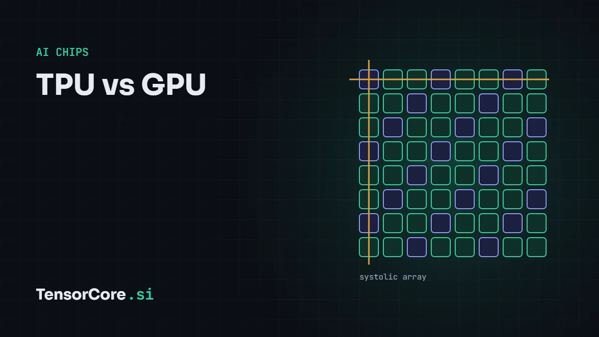
- A TPU has a few very large matrix multiply units (MXUs) built as systolic arrays: grids of multiply-accumulate cells (128 × 128 on several generations, 256 × 256 on Trillium) through which data flows rhythmically, each cell passing its result to its neighbour. A compiler (XLA) plans every data movement in advance.
The systolic design wastes little energy on control logic, so it is very efficient when the work is large, regular matrix math. The GPU design pays a little overhead for flexibility, which helps with irregular workloads, custom kernels and anything that is not a neural network.
TPU vs GPU specs
| Chip | Year | BF16 (dense) | FP8 (dense) | Memory | Bandwidth |
|---|---|---|---|---|---|
| Google TPU v5p | 2023 | 459 TFLOPS | 459 TFLOPS | 95 GiB HBM2e | 2.77 TB/s |
| Google Trillium (v6e) | 2024 | 918 TFLOPS | 918 TFLOPS | 32 GiB HBM | 1.64 TB/s |
| Google Ironwood (TPU7x) | 2025 | 2,307 TFLOPS | 4,614 TFLOPS | 192 GiB HBM3e | 7.38 TB/s |
| NVIDIA H100 SXM | 2022 | 989 TFLOPS | 1,979 TFLOPS | 80 GB HBM3 | 3.35 TB/s |
| NVIDIA B200 | 2024 | 2,250 TFLOPS | 4,500 TFLOPS | 180 GB HBM3e | 8 TB/s |
| AMD MI355X | 2025 | 2,517 TFLOPS | 5,033 TFLOPS | 288 GB HBM3e | 8 TB/s |
Two things stand out. First, raw per-chip throughput is now similar between the best TPU and the best GPUs. Second, NVIDIA and AMD go further down in precision: Blackwell and MI355X run FP4 at roughly double their FP8 rate, while Google does not publish FP4 figures for its TPUs.
Scaling to thousands of chips
Frontier models are trained on thousands of chips, so the network matters as much as the chip. TPUs connect directly to each other through Google's inter-chip interconnect (ICI) in a 3D torus, so an Ironwood pod links 9,216 chips without separate network switches for most traffic. NVIDIA links up to 72 GPUs in one NVLink domain with a GB200 NVL72 rack, at 1.8 TB/s per GPU, and connects racks with InfiniBand or Ethernet. Each approach trades off differently between bandwidth per chip and how many chips share the fastest link.
Software and availability
| GPU (NVIDIA) | TPU (Google) | |
|---|---|---|
| Where to get it | Buy it, or rent from almost any cloud | Google Cloud only |
| Main software | CUDA, PyTorch, TensorRT, vLLM and nearly every AI library | JAX, TensorFlow and PyTorch/XLA, all compiled by XLA |
| Custom kernels | CUDA, Triton, CUTLASS | Pallas (in JAX) |
| Non-AI workloads | Graphics, simulation, FP64 science | Mostly neural networks |
| Local development | Any NVIDIA PC or workstation | Cloud only (small Edge TPUs exist for devices) |
Which should you use?
- Choose GPUs if you need the widest software support, want to run locally or across clouds, use custom CUDA kernels, or run non-AI workloads.
- Choose TPUs if you already work in JAX or TensorFlow, train or serve very large models on Google Cloud, and can benefit from huge pods and Google's pricing for committed use.
- Running models at home? TPUs are not an option; see the best GPU for running LLMs locally.
Frequently asked questions
Is a TPU faster than a GPU?
Not in general. Per chip, Ironwood and B200 are within a few percent on FP8 throughput. Which is faster for a given job depends on the model, the software and how well it maps to each chip, and NVIDIA's Blackwell adds FP4 for inference.
Can I buy a TPU?
Not the data-center kind; Google only offers them as a cloud service. Google's small Edge TPU (sold under the Coral brand) is a separate low-power chip for running small models on devices.
What is the difference between a TPU and an NPU?
NPU (neural processing unit) is a generic name for AI accelerators, usually the small ones built into phones and laptops. TPU is Google's brand name for its own AI chips, mostly the large data-center ones.
Do TPUs have Tensor Cores?
No. "Tensor Core" is NVIDIA's name for its matrix units. A TPU's equivalents are its MXUs (matrix multiply units). Confusingly, Google also calls each compute block of a TPU chip a "TensorCore"; Ironwood has two per chip.
Compare every chip in the GPU specs database, or read B200 vs H100 and GB200 NVL72 explained for NVIDIA's side.

Leave a Reply