 Edited by
Short answer
A GPU is built from many identical blocks called streaming multiprocessors (SMs). Each SM runs thousands of threads in groups of 32 called warps and contains CUDA cores, Tensor Cores, registers and shared memory. Around the SMs sit a large L2 cache and high-bandwidth memory. For AI, the hard part is rarely the math; it is moving data to the Tensor Cores fast enough.
CPU vs GPU: latency vs throughput
A CPU has a handful of large cores built to finish one task as quickly as possible, with deep caches and branch prediction. A GPU takes the opposite approach: thousands of simpler lanes that work on huge amounts of data in parallel. Each lane is slower, but together they finish vastly more work per second when the task can be split up, which is exactly the case for graphics and for neural networks.
Inside a streaming multiprocessor
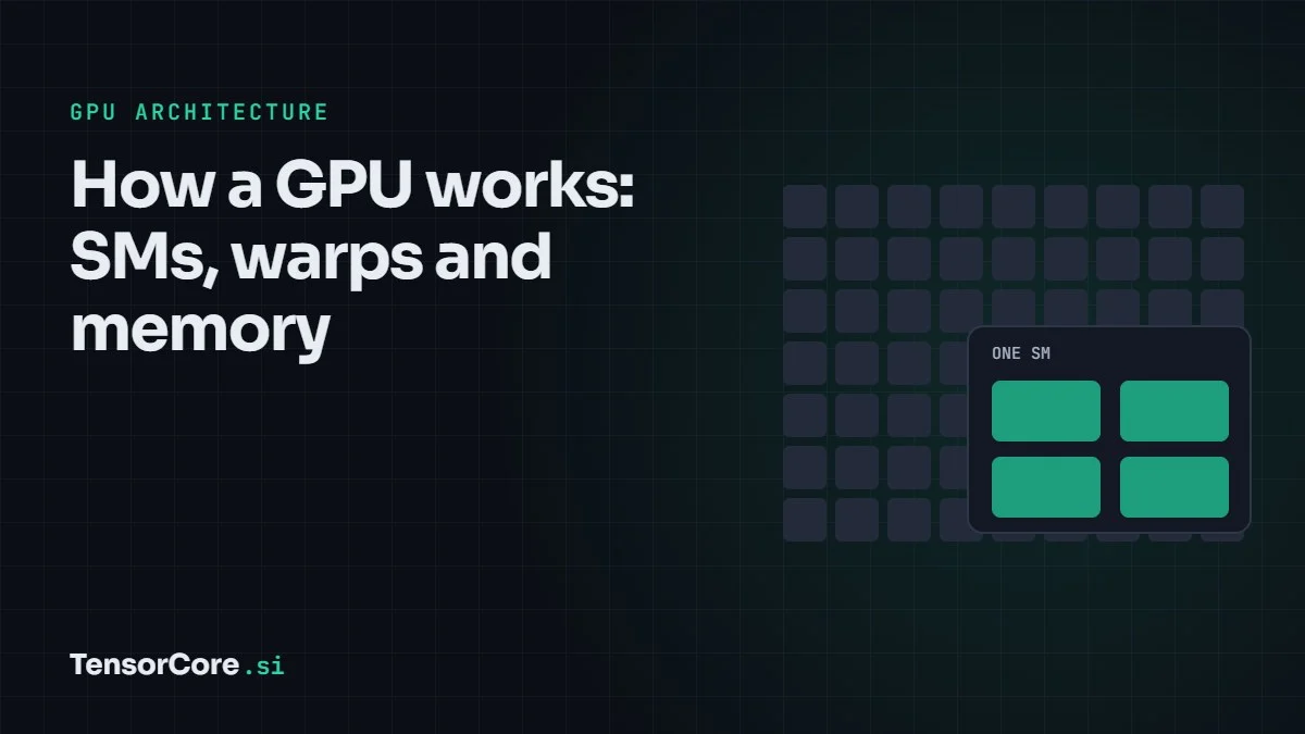
The SM is the GPU's repeated building block. The H100 SXM has 132 of them. Each Hopper SM is divided into four partitions, and each partition contains:
- a warp scheduler that picks which group of 32 threads runs next,
- 32 FP32 CUDA cores (128 per SM) plus integer and FP64 units,
- one Tensor Core for matrix multiply-accumulate,
- a register file of 64 KB (256 KB per SM), the fastest storage on the chip.
The four partitions share up to 256 KB of combined L1 cache and shared memory, plus the Tensor Memory Accelerator that copies tiles in and out. Hover over the exploded chip on our homepage to see how these layers stack up.
Threads, warps and blocks
A GPU program, called a kernel, launches a grid of thread blocks. Each block runs on one SM, and its threads are grouped into warps of 32 that execute the same instruction at the same time on different data. NVIDIA calls this SIMT: single instruction, multiple threads.
An H100 SM can keep up to 64 warps (2,048 threads) resident at once. When one warp waits for memory, the scheduler simply switches to another that is ready, with no cost. This is how GPUs hide memory latency: not by avoiding the wait, but by always having other work to do. Hopper added thread block clusters, which let blocks on neighbouring SMs read each other's shared memory directly.
Tensor Core instructions are issued at warp level, or across a group of four warps on Hopper. Every thread in the warp holds a piece of the A, B and C tiles in its registers, and the Tensor Core combines them.
The memory hierarchy
| Level | Size on H100 SXM | Shared by | Role |
|---|---|---|---|
| Registers | 256 KB per SM | One thread | Operands and accumulators for the current instruction |
| L1 / shared memory | Up to 256 KB per SM | One thread block (or cluster) | Staging area for matrix tiles |
| L2 cache | 50 MB | Whole GPU | Reuse of data across SMs |
| HBM3 | 80 GB at 3.35 TB/s | Whole GPU | Model weights, activations, KV cache |
| NVLink | 900 GB/s per GPU | Other GPUs | Sharing work across a server |
Why data movement decides speed
Divide peak compute by memory bandwidth and you get the ridge point of the roofline model. For H100 SXM in dense FP16: 989 TFLOPS ÷ 3.35 TB/s ≈ 295 floating-point operations per byte. A kernel that does fewer operations than that for each byte it reads from HBM cannot reach peak, no matter how many Tensor Cores it has. It is memory-bound.
Large matrix multiplications are compute-bound, because each loaded value is reused many times. Generating text one token at a time is the opposite: every weight is read once per token for very little math, so speed is set by memory bandwidth. That is why the H200, with the same compute as H100 but 4.8 TB/s of memory bandwidth, generates text noticeably faster. The AI Model Explorer calculates both limits for real models.
attainable FLOPS = min( peak FLOPS, arithmetic intensity × memory bandwidth )
How a matrix multiply flows through the GPU
- The weights and activations sit in HBM.
- The GEMM is cut into tiles, and each thread block is assigned a tile of the output matrix.
- The Tensor Memory Accelerator copies tiles of A and B from HBM, via L2, into shared memory, while the previous tiles are still being computed.
- Warps load fragments into registers (or, on data-center Blackwell, the Tensor Cores read shared memory directly and accumulate into Tensor Memory).
- Tensor Cores run D = A × B + C again and again along the K dimension, building up the accumulator in FP32.
- CUDA cores apply the epilogue: bias, activation function, conversion back to BF16 or FP8.
- The finished output tile is written back to HBM.
Good kernels overlap every step, so Tensor Cores never wait. Libraries such as cuBLAS, cuDNN, CUTLASS and FlashAttention are mostly careful choreography of this pipeline.
From one GPU to thousands
No single GPU can train a frontier model. Servers link 8 GPUs with NVLink (900 GB/s per GPU on Hopper, 1.8 TB/s on Blackwell), and rack-scale systems such as GB200 NVL72 connect 72 Blackwell GPUs into one NVLink domain. Clusters of thousands of GPUs then connect these over InfiniBand or Ethernet. Each level trades bandwidth for scale, the same principle as the memory hierarchy inside one chip.
Next, see how the Tensor Cores themselves evolved in Tensor Core generations, or test yourself on arithmetic intensity and the roofline model in the TensorCore.si Challenge.

Leave a Reply