 Edited by
Short answer
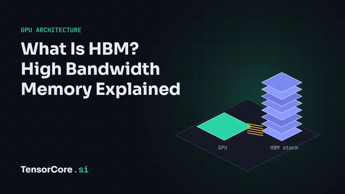
HBM (High Bandwidth Memory) is DRAM built as a vertical stack of memory dies, connected by thousands of through-silicon vias and placed right next to the GPU on the same package. Each stack talks to the GPU over a 1,024-bit-wide bus (2,048 bits for HBM4), which is why an H100 reaches 3.35 TB/s and a B200 8 TB/s. For AI, that bandwidth matters as much as the Tensor Cores: generating text is usually limited by how fast weights can be read from memory.
What HBM is
Every GPU needs memory to hold the data it works on. For an AI model, that means the weights, the activations and, for chatbots, the KV cache that remembers the conversation. Ordinary graphics memory (GDDR) sits in separate chips around the GPU on the circuit board and connects over relatively narrow buses. HBM takes a different approach: it stacks several DRAM dies on top of each other, puts the stack millimetres from the GPU on the same package, and connects it with an extremely wide bus.
The result is far more bandwidth per watt and per square millimetre than any other memory type. HBM was standardised by JEDEC in 2013 and first shipped in AMD's Radeon R9 Fury X in 2015, developed together with SK hynix. Today it is the memory inside almost every data-center AI accelerator, from NVIDIA's H100 and B200 to AMD's Instinct MI355X and Google's TPUs.
How HBM is built
An HBM stack has three key ingredients:
- Stacked DRAM dies. Eight or twelve thin memory dies (16 are allowed in newer standards) sit on top of each other. A 12-high HBM3e stack holds 36 GB.
- Through-silicon vias (TSVs). Thousands of vertical copper connections pass straight through the dies, so every layer can send data down without long wires.
- A base logic die and an interposer. The bottom die manages the stack, and the whole stack sits beside the GPU on a silicon interposer (for NVIDIA GPUs, TSMC's CoWoS packaging) that carries the 1,024 data wires per stack.
Bandwidth per stack is simply the bus width times the data rate per pin. Each pin runs slower than on GDDR memory, but there are far more of them:
bandwidth per stack = bus width (bits) × data rate per pin (Gb/s) ÷ 8
For HBM3 at 6.4 Gb/s per pin: 1,024 × 6.4 ÷ 8 = 819 GB/s per stack. An HBM3e stack at 9.6 Gb/s reaches about 1.2 TB/s, and HBM4 doubles the bus to 2,048 bits for up to about 2 TB/s per stack.
HBM generations
| Generation | First products | Bus per stack | Typical bandwidth per stack | Example GPU |
|---|---|---|---|---|
| HBM | 2015 | 1,024-bit | 128 GB/s | AMD Radeon R9 Fury X |
| HBM2 | 2016 | 1,024-bit | 256–307 GB/s | NVIDIA P100, V100 |
| HBM2e | 2020 | 1,024-bit | about 410–460 GB/s | NVIDIA A100 80GB |
| HBM3 | 2022 | 1,024-bit | up to 819 GB/s | NVIDIA H100, AMD MI300X |
| HBM3e | 2024 | 1,024-bit | about 1.2 TB/s | H200, B200, B300, MI355X |
| HBM4 | 2026 | 2,048-bit | up to about 2 TB/s | NVIDIA Rubin generation |
HBM in AI GPUs
A GPU's total memory bandwidth is the per-stack bandwidth times the number of active stacks. That is why bandwidth jumps when a new GPU adds stacks or moves to a faster HBM generation:
| GPU | HBM type | Capacity | Bandwidth |
|---|---|---|---|
| NVIDIA V100 SXM2 | HBM2 | 32 GB | 0.9 TB/s |
| NVIDIA A100 SXM | HBM2e | 80 GB | 2.04 TB/s |
| NVIDIA H100 SXM | HBM3 | 80 GB | 3.35 TB/s |
| NVIDIA H200 | HBM3e | 141 GB | 4.8 TB/s |
| AMD Instinct MI300X | HBM3 | 192 GB | 5.3 TB/s |
| NVIDIA B200 | HBM3e | 180 GB (HGX) | 8 TB/s |
| NVIDIA B300 / AMD MI355X | HBM3e | 288 GB | 8 TB/s |
Notice that the H200 has exactly the same Tensor Cores as the H100. NVIDIA only changed the memory, from 80 GB of HBM3 to 141 GB of HBM3e, and that alone makes it noticeably faster for large language models.
Why AI needs so much bandwidth
When a chatbot generates text for one user, it produces one token at a time, and each token requires reading every weight of the model from memory once. The math per byte read is tiny, so the Tensor Cores spend most of their time waiting for data. A simple upper bound follows:
max tokens per second (batch 1) ≈ memory bandwidth ÷ model size in bytes
Take an 8-billion-parameter model stored in FP16, about 16 GB. An H100 at 3.35 TB/s tops out near 3,350 ÷ 16 ≈ 210 tokens per second for a single user; an H200 near 300; a B200 near 500. The Tensor Cores barely matter here; memory does. Serving many users at once (batching) reuses each weight for several tokens, which is how servers become compute-bound again. Try it yourself in the AI model GPU calculator or the Roofline Rush game.
Capacity matters too. A 70-billion-parameter model in FP16 needs about 140 GB for its weights alone, more than one H100 holds. That is why 141 GB, 192 GB and 288 GB GPUs are so attractive: fewer GPUs per model means less communication over NVLink.
HBM vs GDDR
| HBM (data center) | GDDR (gaming and workstation) | |
|---|---|---|
| Where it sits | On the GPU package, on an interposer | Separate chips on the circuit board |
| Bus width | 1,024 bits per stack (2,048 for HBM4) | 32 bits per chip; 384–512 bits per GPU |
| Speed per pin | Lower (6.4–9.6 Gb/s for HBM3/3e) | Higher (21 Gb/s GDDR6X, 28+ Gb/s GDDR7) |
| Example total | 8 TB/s on B200 | 1.8 TB/s on GeForce RTX 5090 |
| Cost | High, needs advanced packaging | Much lower |
GDDR wins on cost and is perfect for games, which need less capacity and can tolerate less bandwidth. HBM wins wherever bandwidth and capacity decide performance, which is exactly the situation in large-scale AI.
Costs and limits
- Supply. Only three companies make HBM (SK hynix, Samsung and Micron), and stacking plus advanced packaging capacity has repeatedly limited how many AI GPUs can be built.
- Space. Each stack needs room on the interposer next to the GPU, which caps how many stacks a package can hold, typically six to eight today.
- Heat. Stacking dies makes cooling the lower layers harder, one reason taller stacks arrive slowly.
Frequently asked questions
Is HBM the same as VRAM?
VRAM is a general name for a GPU's own memory. HBM is one type of VRAM; GDDR6, GDDR6X and GDDR7 are others.
Why don't gaming GPUs use HBM?
Cost and packaging. AMD used HBM on some Radeon cards (Fury and Vega), but GDDR delivers enough bandwidth for games at a much lower price, so consumer GPUs moved back to GDDR.
Does HBM matter for training as well as inference?
Yes. Training reuses weights across large batches, so it is more compute-bound than chat inference, but capacity still decides how big a model and batch fit on each GPU, and bandwidth limits optimizer steps, normalization and attention.
What comes after HBM3e?
HBM4, standardised by JEDEC in April 2025, doubles the interface to 2,048 bits per stack. NVIDIA's Rubin generation is built around it.
Keep going with NVLink and NVSwitch explained, compare chips in the GPU specs database, or learn the rest of the chip in how a GPU works.
Sources and further reading
- JEDEC JESD270-4 HBM4 standard and JESD238 HBM3 standard
- NVIDIA H100 and H200 product pages
- NVIDIA HGX B200 and B300 specifications
- AMD Instinct MI300X and MI355X product pages

Leave a Reply