 Edited by
Short answer
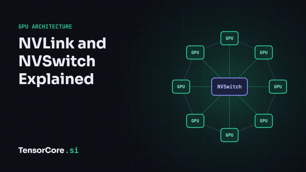
NVLink is NVIDIA's high-speed link between GPUs, and NVSwitch is the switch chip that lets every GPU in a system talk to every other one at full NVLink speed. A Blackwell GPU has 1.8 TB/s of NVLink bandwidth, about 14 times a PCIe Gen5 x16 slot. Large AI models are split across many GPUs, and they have to exchange data after almost every layer, so this bandwidth decides how well a model scales beyond one GPU.
Why GPUs need to talk
A frontier AI model does not fit on one GPU, and even when it does, training it on one GPU would take years. So the work is split, in several ways at once:
- Data parallelism: each GPU trains on different examples, then all GPUs average their gradients (an all-reduce).
- Tensor parallelism: each layer's matrices are split across GPUs, which must combine partial results after every layer.
- Pipeline parallelism: different GPUs hold different layers and pass activations along.
- Expert parallelism: in mixture-of-experts models, tokens are routed to the GPUs that hold the right experts (an all-to-all exchange).
Tensor and expert parallelism move large amounts of data many times per step. If that traffic crawls, the Tensor Cores sit idle waiting for it.
What NVLink is
NVLink is a point-to-point interconnect NVIDIA introduced with the Pascal P100 in 2016. Each GPU has a number of NVLink links, and each link carries data in both directions at once. Compared with PCIe, the general-purpose bus that connects GPUs to the CPU, NVLink offers far more bandwidth, lower latency and support for GPUs reading each other's memory directly.
For context, a PCIe Gen5 x16 slot moves about 64 GB/s in each direction (128 GB/s both ways). An H100's NVLink moves 900 GB/s, which NVIDIA describes as about 7 times PCIe Gen5.
NVLink generations
| Generation | GPU | Year | Links per GPU | Total bandwidth per GPU |
|---|---|---|---|---|
| NVLink 1 | Pascal P100 | 2016 | 4 | 160 GB/s |
| NVLink 2 | Volta V100 | 2017 | 6 | 300 GB/s |
| NVLink 3 | Ampere A100 | 2020 | 12 | 600 GB/s |
| NVLink 4 | Hopper H100 / H200 | 2022 | 18 | 900 GB/s |
| NVLink 5 | Blackwell B200 / B300 | 2024 | 18 | 1.8 TB/s |
| NVLink 6 | Rubin (announced) | 2026 | – | 3.6 TB/s |
NVSwitch and NVL72
Direct links only go so far: with 18 links, a GPU can connect to a handful of neighbours, and traffic between distant GPUs has to hop. NVSwitch solves this. It is a switch chip, first used in the DGX-2 in 2018 to connect 16 V100s, that gives every GPU a full-speed path to every other GPU.
- HGX H100 and HGX B200 servers connect 8 GPUs through NVSwitch chips on the baseboard, so any pair communicates at full NVLink speed.
- GB200 NVL72 extends the NVLink domain to a whole rack: 72 Blackwell GPUs and 36 Grace CPUs, linked through NVLink switch trays, with about 130 TB/s of total NVLink bandwidth (72 × 1.8 TB/s).
Inside one NVLink domain, software can treat the GPUs almost like one giant accelerator. This is why rack-scale systems are attractive for mixture-of-experts models, whose all-to-all traffic punishes slower links.
How much time does communication cost?
The most common operation is the ring all-reduce, used to sum gradients across GPUs. Each GPU sends and receives about twice the data size:
data sent per GPU = 2 × (N − 1) ÷ N × data size
Say 8 GPUs must all-reduce 1 GB of FP16 gradients. Each GPU sends 2 × 7 ÷ 8 × 1 GB = 1.75 GB. With H100 NVLink at 450 GB/s in each direction, that takes about 3.9 ms in the ideal case. Over PCIe Gen5 at 64 GB/s per direction it would take about 27 ms, roughly seven times longer, and that cost repeats every training step.
Real all-reduces add latency and protocol overhead, and libraries such as NVIDIA's NCCL overlap communication with computation to hide some of it. The ratio, though, is why NVLink exists.
Beyond one rack: InfiniBand and Ethernet
Training clusters link thousands of GPUs, far beyond one NVLink domain. Between servers and racks, each GPU typically gets its own network card, such as a 400 Gb/s (50 GB/s) InfiniBand or Ethernet adapter, or an 800 Gb/s one on newer systems. That is still an order of magnitude below NVLink, so engineers keep the chattiest traffic (tensor and expert parallelism) inside the NVLink domain and send lighter traffic (data and pipeline parallelism) across the network.
| Link | Bandwidth per GPU (each direction) | Typical reach |
|---|---|---|
| HBM3e (on package) | 8,000 GB/s total | One GPU |
| NVLink 5 | 900 GB/s | 8 to 72 GPUs |
| PCIe Gen5 x16 | 64 GB/s | GPU to CPU |
| 400 Gb/s InfiniBand or Ethernet | 50 GB/s | Whole cluster |
AMD, Google and open standards
- AMD connects Instinct GPUs with Infinity Fabric links, about 896 GB/s of total bandwidth per MI300X.
- Google TPUs use their own inter-chip interconnect (ICI); an Ironwood TPU has 1.2 TB/s of bidirectional ICI bandwidth, and pods reach 9,216 chips.
- UALink, an open accelerator-interconnect standard backed by AMD, Intel, Google, Microsoft, Meta and others, was formed in 2024 as an industry alternative to NVLink.
Frequently asked questions
Do gaming GPUs have NVLink?
Some older ones did, through a bridge between two cards (the GeForce RTX 3090 was the last). The RTX 40 and 50 series dropped NVLink, so consumer multi-GPU setups now communicate over PCIe.
Is NVLink needed for inference?
If a model fits on one GPU, no. Once a model is split across several GPUs with tensor parallelism, NVLink makes a large difference to latency, because partial results are exchanged after every layer for every token.
What is NVLink-C2C?
A chip-to-chip version of NVLink that connects NVIDIA's Grace CPU to a Hopper or Blackwell GPU at 900 GB/s with coherent memory, so the GPU can use the CPU's memory far faster than over PCIe.
Next, see why on-package memory is even faster in what is HBM, compare interconnects in the GPU specs database, or learn to decode every line in how to read a GPU spec sheet.

Leave a Reply